Since we are dealing with RF we have to keep it away from all other components and equipment in our shack. The only thing you want to generate or pick-up RF with is your antenna. In our case a magnetic loop antenna.
The purpose of the SWR Bridge, or tandem match, is to measure the difference between the forwarded and reflected power. To do that, we have to place the SWR Bridge between our antenna and our transceiver. Ideally, this should be done as close as possible to the antenna. This, however, is not very practical, as you won’t be able to read the values on the screen.
That’s why its placed inside the automatic magnetic loop controller unit and also why we need to create a shield that will keep the RF inside the SWR Bridge box.
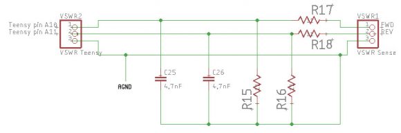
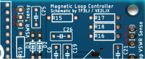
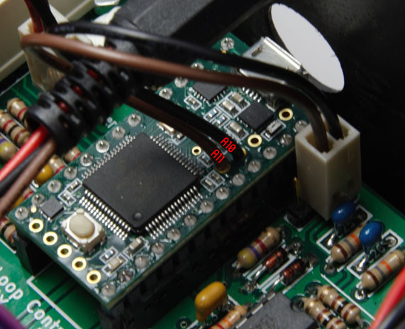
To be able to measure the differences between forward and reflected power, we need to connect the SWR Bridge to the Teensy, pad A10 and A11. If we would just drill two holes in the tinned box and wired the SWR Bridge directly to the Teensy, the RF could still escape and cause trouble in our tuner or even in the shack. By using feed through capacitors, we can connect the SWR Bridge to the Teensy and measure both forward and reflected power, while still keeping the RF in the shielded box.
Let’s zoom in on the electric diagrams, the source code and the PCB design to know how the SWR Bridge must be connected to the Automatic Magnetic Loop Controller PCB’s. This implies both Loftur as mine PCB designs.
From the ML.h file:// AD inputs for Forward and Reflected Power (SWR measurement)
const int Pfwd = A10;
const int Pref = A11;
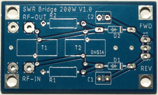
Looking at the SWR Bridge, or Sontheimer Bridge, it’s fairly easy to understand. Connect your transceiver to RF In, connect the antenna to RF Out. On the other side of the board, we have FWD (pin 1), GND (pin 2) and REF (pin 3). This is the part where we need to keep attention. On the PCB the pinout position is different for GND and REF.
Connect SWR Bridge pin 1 (FWD) with pin 1 on the PCB, SWR Bridge pin 2 (GND) with pin 3 on the PCB and SWR Bridge pin 3 (REF) with pin 2 on the PCB. After our signals went through some resistors and capacitors, they can be connected via another 3 pin header to the Teensy 3.2 pads A10 and A11. Pin 1 (FWD) is connected to Teensy pad A10, and pin 2 (REF) to Teensy pad A11.
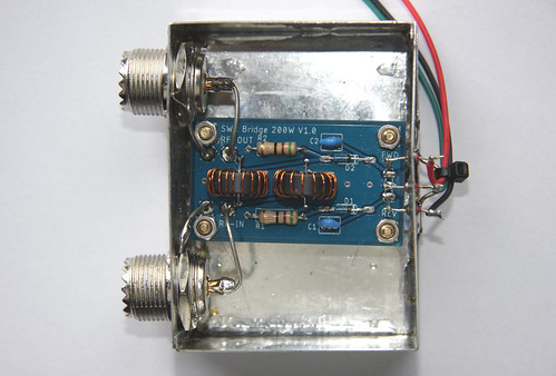

Are you using any type of capacitor between the FWD/REV on the SWR board and the main board? Looks like there is something there.
Hello Paul, I’m using feedthrough capacitors of 1000 pF. This way we can keep the RF inside the box and still read the voltage differences between FWD and REV.
Hello! I’m in the process of getting on of these together and have my mainboard design complete, but have a couple of questions:-
1. Do you recall the dimensions of your SWR Bridge board that I could use as a starting point? I can’t find any reference anywhere either for your board or the one done by Kits and Parts.
2. Instead of “overhead wires” from A10 and A11 of the Teensy to a header connector I have just incorporated tracks on the main PCB since looking at the Teensy 3.2 Development Board used there seem to be no reason why a set of header pins can’t be added alongside the other pins to plug in A10 and A11 at the same time. DO you foresee any problem with that?
3. Paul Gaffney (above) made reference to what you said are “feedthrough capacitors”. I can’t seem to locate them anywhere. Could you explain where they are and what voltages the 1000 pF caps are?
Thank you!
Hello Richard,
1) the SWR bridge PCB’s measure 48,6 mm x 28,6 mm
2) that’s certainly worth a try. I assume you have the tracks of the main pin header on the top and the tracks to A10 and A11 on the bottom of the PCB? The question is if the spacing between top and bottom copper is enough. For our pupose, probably yes.
3) That’ a tricky one. Here’s some info about what feedthrough capacitors are: https://www.hobbyprojects.com/electronics_component_symbols/what_is_feedthrough_capacitor.html?no_redirect=true I always buy mine at local ham fairs. They don’t need to have a high voltage rating as the A10 and A11 only expect +- 3.3V max.
Hello Frederik
Thanks for getting back to me with that info. I actually have the tracks to A10 and A11 (pins 31 and 32 on the Teensy Development Board) on the top layer of the main PCB. I suspect you’re going to say that’s a problem? Moving them to the other side would be easy enough but why? The proximity of those pins to the others on the Teensy board is pretty close anyway. Perhaps I’m failing to understand the theory in all this?
When I asked about the feedthrough caps it was because Paul Gaffney had said “Looks like there is something there”, and I couldn’t see anything in your photos. Where exactly are they located?
Many thanks!
Hello Richard,
I don’t think it matters on which layer the tracks are, as long as they don’t cross other tracks. I thought it was a difficult spot to reach (as it’s in the middle of the Teensy) and using overhead wires made it easy to overcome this issue.
I’ve annotated the picture on flickr to show where the feedthrough capacitors are: https://www.flickr.com/photos/golb-be/40749031832/in/album-72157694013561054/ They are placed in the holes where the wires would leave the RF box and are used to keep the RF in the box but to let the DC reach the A10 and A11 pin.
Hello Frederik,
No, the tracks on my PCB design are clear of each other. I used Kicad to ensure there were no potential problems.
I now see where you placed the feedthrough caps. I had totally missed those before.
Thank you so much for taking time to clear up my questions. You’ve been a great help!